15 5 月 Press release: Trymax Receives Multi-System Orders from a Top 10 Semiconductor Packaging House
Multi-site shipment in Taiwan and China for 200mm and 300mm bumping descum solutions.
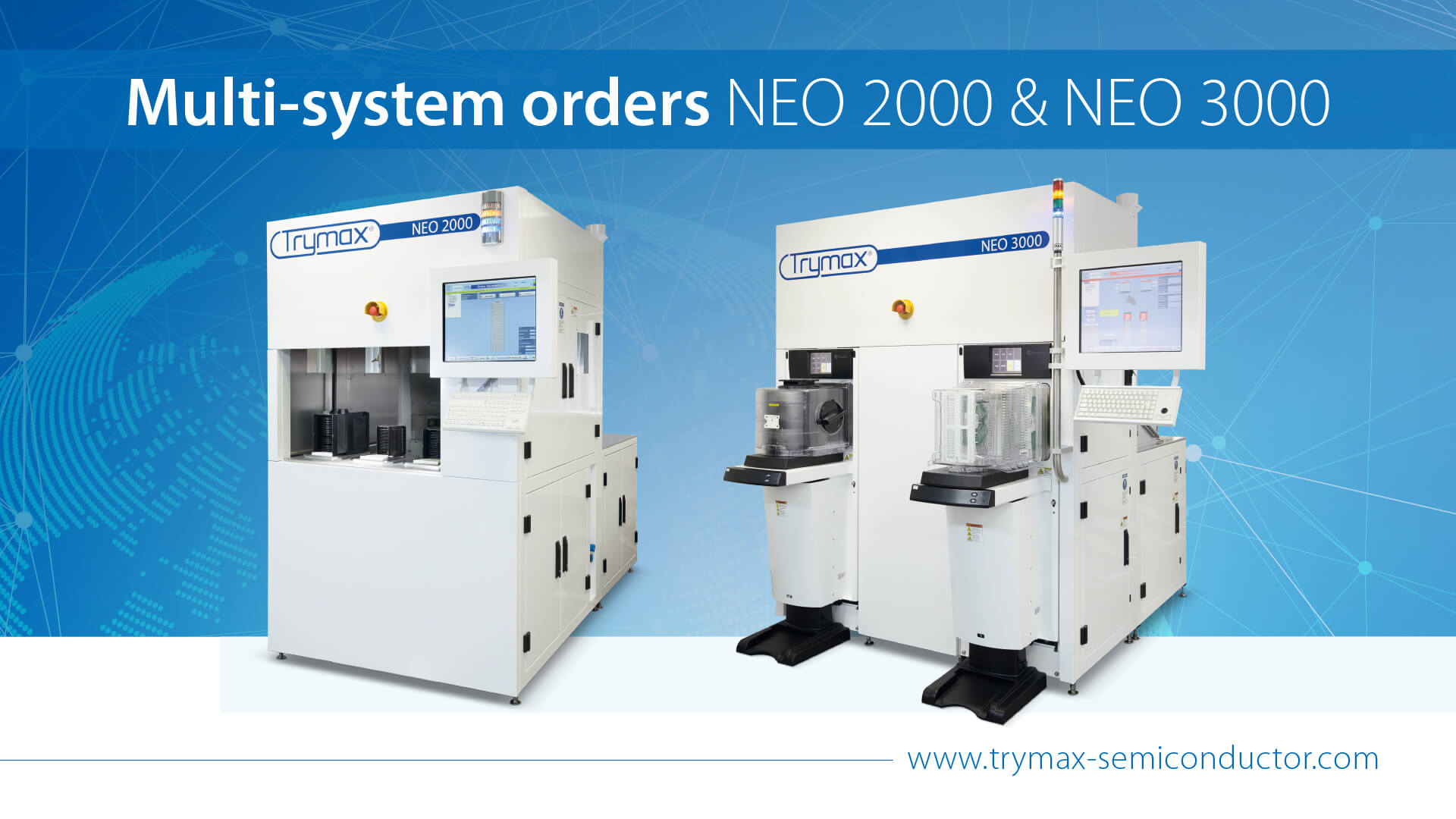
NIJMEGEN, THE NETHERLANDS – May 15, 2019. Trymax Semiconductor Equipment BV (Trymax), a global leader in plasma solutions, today announced it has received multi-system orders for its NEO 2000 and NEO 3000 series from a leading Taiwanese packaging house. This order will expand the existing NEO install base at the customer in Taiwan and allows Trymax to break into the customer’s fab in China. Shipping of the systems will start in Q2 and continue during Q3 2019.
“We are pleased to receive this order for several shipments in two different fabs”, said Jonathan Lee, General Manager of Trymax in Asia. “Many companies claim to deliver the best Cost of Ownership but these repeat and expansion orders are a concrete example that our solutions are truly delivering it”.
NEO 2000 series is a dual chamber system for wafers up to 200mm. NEO 3000 series is a dual chamber system for wafers up to 300mm. All systems will be configured with Trymax’s dual source plasma technology combining RF and microwave to provide the best ashing rate and uniformity trade-off. The dual source technology is the choice recommended by Trymax for many wafer level packaging applications such as bumping or Fan-Out Wafer Level Packaging.
This month, Trymax will be sponsoring the Plasma Etch and Strip in Microtechnology workshop (PESM) in Grenoble (France) in May 20-21, and the SEMI Fab Owner Alliance meeting in Lowell (USA) in May 22-23. Trymax will be exhibiting at the Electronic Components and Technology Conference (ECTC) in Las Vegas (USA) in May 28-31. Staff of the company can be met at these events to learn more about NEO series.
About Trymax Semiconductor Equipment BV:
Trymax’s core business is to support semiconductor manufacturers through the world with innovative plasma-based solutions for photo resist removal, surface cleaning, isotropic etch, as well as UV curing/charge erase, that are used in the fabrication of integrated circuits and other semiconductor devices. Trymax is a privately held company headquartered in Nijmegen, The Netherlands. Trymax operates regional offices in China (Suzhou) and Italy (Milan). Learn more at www.trymax-semiconductor.com.
Company contact:
Yann Guillou
Global Marketing & Sales Director
+31 24 350 08 09
[email protected]